
In the lead-free wave soldering, there are many bad wave soldering phenomena caused by the through-hole problem of the circuit board. What are the specific ones? It is estimated that many small partners do not know, the wave soldering manufacturer Guang Shengde focuses on analyzing the reasons for this.
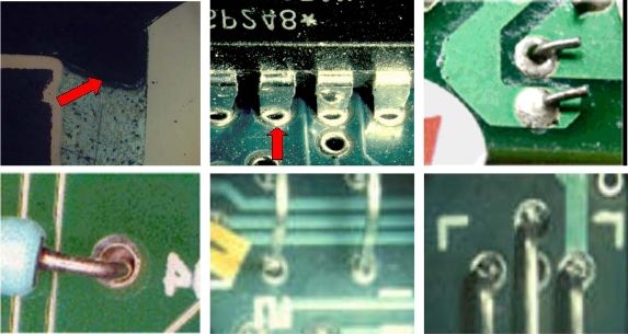
Poor through hole on the circuit board
1. The preheating temperature is too low or too high to cause poor or loss of activity of the flux, uneven flux coating, insufficient fluxing effect on the pads, component pins, and through holes, which directly affects the solder on the surface Of wetting and spreading.
2. Insufficient wave crest height and too large guide rail inclination angle: Insufficient wave crest height or too large guide rail inclination angle will directly cause the capillary action of the solder to drop in the climbing height, insufficient solder on the wave crest to press into the hole, and shorten the contact time between the solder and the pad. A large proportion of through holes are formed.
3. The circuit board pad, through-hole plating or the surface of the component pin is contaminated and oxidized, resulting in poor solderability, difficulty in climbing solder during the soldering process or decreased wettability of the solder to the pad, resulting in sinking copper holes and pad parts Not tin.
4. The wave soldering chain speed is too fast, the PCB and the wave crest contact time is not enough; the chain jitter is large, and the soldering process is not stable enough.
5. The aperture of the through hole does not match the diameter of the component pin: after the component is inserted, if the pin gap in the via hole is too small, the solder cannot climb to the component surface in a short time. Directly cause the solder to fall back into the tin furnace.
6. Pad offset: When the pad deviates from the center of the via hole, the large part of the pad is similar to the thief pad, so the solder at the narrow part of the pad is gathered to the wider part of the pad.
7. Components whose lead-out surface is flat are attached to the board for insertion: the hot air released from the PCB hole wall during wave soldering cannot flow out from above, and the hot air is discharged from below the solder joints, resulting in through-hole defects.
8. Excessive flux spraying amount of lead-free wave soldering machine or PCB moisture content exceeds the standard, this kind of through hole is caused especially on the PCB with poor substrate material (for example, the plate is CM-1) or the rougher drilling method is used. It is more common that the flux cannot be completely volatilized and overflowed before soldering. The steam that evaporates from the moisture forms a high-pressure effect, and the steam overflows mainly at the aperture, and then forms a pinhole-like poor soldering phenomenon. The through-holes caused by this reason are usually in the board. The surface is accompanied by the formation of tin beads.
9. Poor punching of vias, burrs in the holes, jagged copper chips on the edges, and unsmooth pads, resulting in a decrease in the surface tension of the solder, and the solder fails to grasp the component pins and pads, resulting in through-hole defects.
 Website QR code